Skin Depth and Wall Thickness for Copper Induction Coils, Busbars and RF Parts
How to estimate copper skin depth at your operating frequency, size conductor walls and plating from it, and decide when printed wall thickness or surface roughness starts to change AC losses.
Working on a copper part? Start a project review — share a brief; CAD can follow.
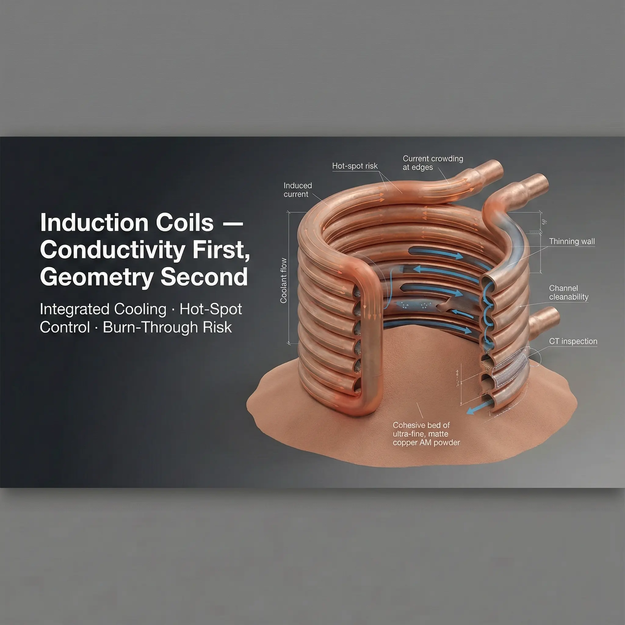
At alternating current, copper only conducts well in a thin layer at the current-carrying surface. That layer, the skin depth, is about 9 mm at 50 Hz, about 0.66 mm at 10 kHz, about 66 µm at 1 MHz and well under 1 µm at 10 GHz for standard annealed copper at 20 °C. Size the conducting wall from it: induction-heating references put the electrically effective coil wall at roughly 1.6 to 2 skin depths. In the low-kilohertz induction range, wall thickness is a real electrical decision; at higher induction frequencies the mechanical wall governs; in RF parts, surface roughness and plating decide the losses.
This guide is for engineers specifying copper induction coils, high-current conductors and RF or microwave parts that may be made by laser powder bed fusion (LPBF) or conventionally. It answers one question: at a given frequency, how thick does the copper need to be, and when does the printed wall or printed surface start to change AC losses?
What it cannot settle without your inputs: the operating frequency (or harmonic spectrum), the delivered conductivity of the actual copper grade and state, the operating temperature, which surface carries the current, and the pressure and mechanical loads on the same wall. For commercial reviews, see the induction coil, busbar and RF waveguide pages.
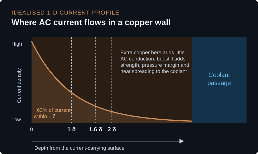
Cover: a reused reference illustration from this site’s image library, not a photograph of a specific part or test. The current-profile diagram below is an original explanatory drawing of an idealised one-dimensional case, not a simulation.
Quick decision table
| Frequency range (examples) | Copper skin depth, 100% IACS, 20 °C | What usually limits the design | Printing relevance |
|---|---|---|---|
| 50–60 Hz power | ~9.3–8.5 mm | Cross-section, temperature rise, joints | Only for geometry or integrated cooling |
| 1–10 kHz induction | ~2.1–0.66 mm | Coil wall vs cooling bore vs pressure | Wall can be sized to frequency |
| 100 kHz–1 MHz induction / power | ~0.21–0.066 mm | Mechanical wall, not electrical wall | Surface condition starts to matter |
| 13.56 MHz–1 GHz RF | ~18–2.1 µm | Surface finish, plating, contacts | As-built roughness exceeds skin depth |
| 3–30 GHz microwave | ~1.2–0.38 µm | Surface roughness and surface chemistry | Finishing route decides the loss |
Read the table as a screening tool. It tells you which question to ask first; it does not size a part.
How to calculate copper skin depth
For a good conductor with a flat or large-radius surface, the skin depth is:
δ = √( ρ / (π · f · μ₀ · μᵣ) )
where ρ is resistivity (Ω·m), f is frequency (Hz), μ₀ = 4π × 10⁻⁷ H/m and μᵣ ≈ 1 for copper. Skin depth falls with the square root of frequency and rises with the square root of resistivity. MIT’s 6.013 electromagnetics text gives this dependence and notes that for good conductors δ runs from about 1 cm at 60 Hz to less than 0.1 mm at 1 MHz.
For the reference resistivity we use the International Annealed Copper Standard: 100% IACS corresponds to 0.017241 Ω·mm²/m at 20 °C, with a temperature coefficient of 0.00393 per °C for standard annealed copper, as recorded in NBS Handbook 100, Copper Wire Tables.
Reference values
Calculated from the formula above with ρ = 1.7241 × 10⁻⁸ Ω·m (100% IACS, 20 °C) and μᵣ = 1:
| Frequency | Skin depth δ | 1.6 δ | 2 δ |
|---|---|---|---|
| 50 Hz | 9.35 mm | 14.95 mm | 18.69 mm |
| 60 Hz | 8.53 mm | 13.65 mm | 17.06 mm |
| 1 kHz | 2.09 mm | 3.34 mm | 4.18 mm |
| 3 kHz | 1.21 mm | 1.93 mm | 2.41 mm |
| 10 kHz | 0.66 mm | 1.06 mm | 1.32 mm |
| 30 kHz | 0.38 mm | 0.61 mm | 0.76 mm |
| 100 kHz | 0.21 mm | 0.33 mm | 0.42 mm |
| 400 kHz | 105 µm | 167 µm | 209 µm |
| 1 MHz | 66 µm | 106 µm | 132 µm |
| 13.56 MHz | 18 µm | 29 µm | 36 µm |
| 1 GHz | 2.1 µm | 3.3 µm | 4.2 µm |
| 10 GHz | 0.66 µm | 1.06 µm | 1.32 µm |
These are reference calculations, not properties of any delivered part. Three corrections change them in practice:
- Lower conductivity makes δ larger. δ scales with √ρ. A copper at 80% IACS has a skin depth about 1.12 times the table value, and its surface resistance is higher by the same factor. Use the measured conductivity of the delivered material state, not the powder grade; see electrical conductivity in 3D printed copper parts.
- Temperature makes δ larger. Using the 0.00393/°C coefficient, standard annealed copper at 80 °C has about 24% higher resistivity than at 20 °C, so δ is about 11% larger. A coil wall that runs hot also loses more.
- Geometry and neighbours redistribute current. The formula assumes a flat surface carrying current on one side. Thin wires, sharp edges, adjacent turns and return conductors (proximity effect) move current to particular faces. The formula gives the depth scale, not the distribution.
Wall thickness for induction coils
In a large conductor, Fluxtrol’s inductor design reference notes that about 63% of the current and 86% of the power sit within the first reference depth. The same source treats a conducting wall of about 1.6 δ as the most effective thickness from a one-dimensional analysis, says thinner walls reduce coil efficiency, and notes that walls are often much thicker for mechanical reasons. Ambrell’s coil design guide uses 2 δ as the theoretical tubing wall and notes that walls thinner than 2 δ are often used with only a nominal efficiency loss.
Treat 1.6–2 δ as the electrical starting point for the wall between the current-carrying face and the coolant. Then check three things the electrical rule ignores:
- Mechanical and pressure margin. At 100 kHz and above, 2 δ is a fraction of a millimetre. The wall must still survive coolant pressure, bending, clamping, handling and thermal cycling. Here the mechanical wall decides, and the electrical rule is automatically met.
- Heat path to the coolant. Coil losses plus heat radiated from the hot workpiece have to cross the wall. The Fluxtrol reference describes a case in which a thin wall with low-pressure water ran hot enough at the water side to risk vapour blanketing and short coil life. A thicker wall is not always cooler, and a thinner wall is not always more efficient; the coolant side has to be designed with the wall.
- Which face carries the current. In a coil, current concentrates on the face toward the workpiece. Wall thickness matters most there. Other faces can be sized for strength and printability.
What changes when the coil is printed
LPBF lets the wall vary around the cross-section. A designer can keep about 2 δ on the heating face, thicken the outer faces for stiffness, and shape the coolant passage to follow the heating face. That is a real design freedom, but it creates verification questions:
- Minimum printable and inspectable wall. A wall that is electrically adequate at 400 kHz may be too thin to print, clean and pressure-test reliably. Agree a minimum wall from the supplier’s process data and your proof-pressure requirement, not from the δ table.
- Material state. Conductivity after printing and heat treatment sets the real δ and the losses. Define the grade and final state, and ask for conductivity measured on that state.
- Surface on the heating face. At high induction frequencies the as-built surface is a large fraction of δ; machining or finishing that face may matter more than wall thickness.
For the wider coil decision, including joints, published service-life results and qualification, see copper induction coils: traditional manufacturing vs 3D printing.
Busbars and power conductors at 50/60 Hz
At mains frequency, copper’s skin depth is about 8.5–9.3 mm. Two consequences follow:
- Thin bars are barely affected. In a bar a few millimetres thick, current spreads almost evenly through the section, and DC resistance is a reasonable first estimate.
- Very thick solid sections are inefficient at AC. Once a dimension is well beyond about 2 δ (roughly 17–19 mm), the centre carries little current. Designers typically split the conductor into laminations, use a hollow or channel section, or add cooling rather than add more solid copper.
Real AC/DC resistance ratios depend on bar shape, spacing and phase arrangement, and are tabulated in busbar design references such as the Copper Development Association’s Publication 22, Copper for Busbars. Use those methods or a field simulation for ratings; this article does not provide current ratings.
Harmonics matter. Power electronics put current at multiples of the switching or fundamental frequency, where δ is much smaller. A busbar fed by an inverter may need to be checked at the harmonic frequencies that carry significant current, not only at 50/60 Hz.
When is a printed or custom conductor worth it? Mainly when the conductor must also carry coolant, follow a three-dimensional path, or merge several joints. A printed busbar is not usually justified by skin effect alone; a laminated or hollow conventional section often solves that more cheaply. For the busbar RFQ side, use the custom copper busbar page.
RF and microwave parts: surface first, wall second
At RF frequencies δ is a few micrometres or less. Any practical printed wall is hundreds of skin depths thick, so the wall-thickness question disappears. Two other questions replace it.
Surface roughness relative to skin depth
When roughness becomes comparable to or larger than the skin depth, current follows a longer, rougher path and conductor loss rises. Horn, Reynolds and Rautio summarise the classical roughness correction, which reaches a maximum of a factor of two, and then report measurements on copper-foil microstrip lines showing increases larger than that factor, with no saturation up to 50 GHz (IEEE IMS 2010 paper). Those were rolled or electrodeposited foils on circuit laminates, not printed parts, but the mechanism is the same.
For LPBF copper, published third-party results show the scale of the effect. Mayerhofer et al. printed pure-copper 4.26 GHz single-cell cavities with red and green lasers. Skin depth there is about 1 µm. As printed, the average unloaded quality factor was about 42% (red laser) and 22% (green laser) of the simulated value, which the authors mainly attribute to surface roughness extending over several skin depths. After chemical post-processing that removed tens to over a hundred micrometres of material, quality factors rose substantially, with the best cavities approaching the simulated value (Instruments 2024, 8, 39, open access). These are the authors’ results for their geometry, machines and finishing route; they are not COPPER 3DP test data and do not set a limit for other parts.
Plating thickness
If an RF surface is plated (for example silver over copper), the same δ formula applies to the plating metal at the operating frequency. A plating that is only a fraction of its own skin depth leaves part of the current in the layer below, so plating thickness, coverage inside internal passages and the substrate surface underneath all matter. Specify plating by the RF-critical zones and verify the delivered part by RF measurement; surface zoning and plating are covered in copper AM waveguide surface finish and plating by frequency band.
Performance vs acceptance
Keep reference values and drawing requirements separate.
| Item | Reference value (screening) | What the drawing or purchase order should state |
|---|---|---|
| Skin depth | Table above, 100% IACS, 20 °C | Not specified; it follows from frequency and material |
| Conductivity | 100% IACS is a definition, not a printed-part value | Minimum conductivity, method, temperature, specimen location, material state |
| Conducting wall | 1.6–2 δ at operating frequency (induction references) | Minimum wall on named faces, with inspection method |
| Mechanical wall | Not set by skin depth | Design and proof pressure, leak test and acceptance |
| RF surface | Loss rises when roughness ≳ δ | Finish route per zone, plating spec, final RF test (loss, Q, return loss) |
| Hot operation | δ and loss rise with temperature | Operating temperature and coolant conditions for any performance test |
A conductivity coupon proves the material state, not the hidden wall. A pressure test proves the wall holds, not that it is electrically efficient. The final functional test, a heating trial, a temperature-rise test or an RF measurement, is what integrates them.
When printing is the wrong answer
- A tube or bar already gives the right section. If standard copper tube with a wall near 2 δ meets the coil shape and cooling, keep it; Ambrell’s guide notes that available tube walls are often thinner than 2 δ without serious penalty.
- The problem is a thick solid conductor at 50/60 Hz. Laminated, hollow or channel sections are the established fix.
- The RF surface cannot be reached. If an internal RF surface cannot be machined, polished, chemically finished or plated, and as-built roughness exceeds several skin depths, expect higher loss. A machined split-block or electroformed part may be the better route.
- Strength dominates. If the part needs more strength or softening resistance than pure copper offers, a copper alloy such as CuCrZr changes the trade-off. It has lower conductivity, so its skin depth and losses are higher. Compare them at the operating temperature.
- Volume is high and geometry simple. Drawn tube, extruded bar and machined parts are cheaper and well characterised.
RFQ checklist
Send what you have and mark unknowns as pending:
- CAD and drawing, with the current-carrying faces and RF-critical surfaces identified.
- Operating frequency or frequency range; for inverter-fed parts, significant harmonics.
- Current (RMS and peak), duty cycle, and power if known.
- Copper grade and required final state; minimum conductivity and how it is to be measured.
- Operating temperature range and coolant, inlet temperature, flow and allowable pressure drop.
- Design and proof pressure, leak test method and acceptance.
- Minimum wall required on named faces, and whether it is electrical, mechanical or both.
- Surface requirements per zone: as-built, machined, polished, chemically finished or plated; plating metal and thickness.
- Functional acceptance: heating trial, temperature-rise test, DC/AC resistance or RF measurement, and who performs it.
- Quantity, prototype and repeat-build plan, and target date.
Submit through the secure RFQ form. We review the frequency, wall, cooling and surface requirements together and say which ones the printed route can and cannot meet before quoting.
Sources and scope
Sources were reviewed on 28 October 2026. Skin-depth values in the tables are our calculations from the standard formula with the NBS Handbook 100 annealed-copper resistivity; they are reference values for flat, single-sided conduction at 20 °C, not measured properties of any part. Wall-thickness rules of thumb come from the cited induction-equipment references and are design starting points. The roughness and RF-cavity results are published third-party research on the stated materials and conditions; they are not COPPER 3DP projects or test data. No current ratings, tolerances, conductivity guarantees or prices are given here.
- National Bureau of Standards, Handbook 100, Copper Wire Tables (1966): IACS resistivity and temperature coefficient.
- Haus and Melcher, Electromagnetic Fields and Energy, MIT 6.013, section 10.7: skin-depth dependence on frequency and conductivity.
- Fluxtrol, Design and fabrication of inductors for induction heat treating: current and power within the reference depth; 1.6 δ wall; cooling-side risk.
- Ambrell, Complete Guide to Induction Coil Design: 2 δ theoretical tubing wall.
- Horn, Reynolds and Rautio, Conductor profile effects on the propagation constant of microstrip transmission lines, IEEE IMS 2010: roughness and conductor loss.
- Mayerhofer et al., Red and green laser powder bed fusion of pure copper in combination with chemical post-processing for RF cavity fabrication, Instruments 2024: LPBF copper cavity Q before and after finishing.
Copper AM quotation
Is copper AM a fit for your part?
Describe the part, its job, and the question holding up your decision. Add quantity and critical requirements if known; CAD can follow.
NDA available on request. We reply within 2 business days.
Before you submit: Copper AM capabilities and review scope.