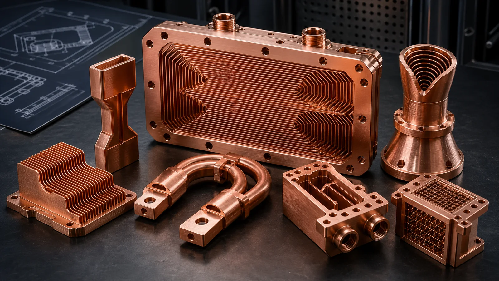
Pure Copper Additive Manufacturing for Conductive Components
A practical RFQ guide to pure copper additive manufacturing for conductive components, covering contact pads, current path geometry, connector bodies, busbar blocks, electrodes, surface finish, plating, and conductivity evidence.
Working on a copper part? Start a project review — share a brief; CAD can follow.
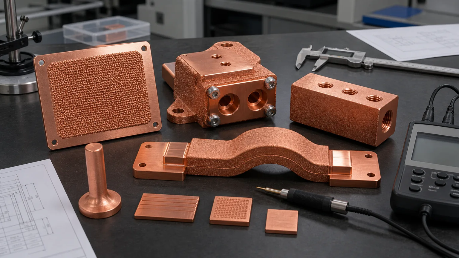
Pure copper additive manufacturing is useful for conductive components when the electrical function and the geometry both matter. The strongest candidates are not simple copper rectangles. They are contact blocks, connector bodies, busbar transitions, electrodes, induction coil segments, power distribution parts, and cooled conductors where current path, surface finish, assembly interfaces, and validation evidence must be reviewed together.
This guide is intentionally narrow.
It is not a general introduction to pure copper 3D printing. It is also not a broad explanation of electrical conductivity in 3D printed copper parts. This page focuses on conductive components as quoted hardware: where current enters, where it leaves, how the current path changes shape, what surfaces must be machined or plated, how contact resistance is controlled, and what evidence should be requested before the part is accepted.
Why Pure Copper AM Appears In Conductive Component RFQs
Pure copper is attractive because it offers high electrical conductivity and high thermal conductivity. That makes it a natural material to review for conductors, contact blocks, electrodes, induction hardware, RF surfaces, and compact power components.
Industrial material suppliers point in the same direction. EOS describes copper AM materials around strong electrical and thermal conductivity, with application families that include electronics, heat exchangers, motors, inductors, coils, and other parts where copper’s conductivity is the main reason for using the material. Eplus3D lists pure copper and CuCrZr for heat exchangers, induction coils, high-frequency electronics, molding, tooling, and electronics. 3D Systems’ oxygen-free copper material page connects printed copper to conductive applications such as bus bars, coils, antennas, RF shielding, waveguides, and heat exchangers.
Those signals are useful, but they should not be turned into a blanket promise. Conductive copper components fail or pass as finished parts, not as keywords. A high-conductivity powder route does not guarantee a low-resistance joint, a flat contact pad, a clean cooling channel, or a stable threaded terminal.
For RFQ work, the useful question is:
Can this pure copper component be printed, cleaned, machined, finished, and tested so the final current path and contact interfaces meet the application requirement?
Where Pure Copper AM Is A Strong Candidate
Pure copper additive manufacturing is most valuable when a conductor needs geometry that conventional copper fabrication handles poorly.
Good candidates include:
- Connector bodies with complex current routing, integrated mounts, or compact packaging.
- Contact blocks with machined pads, cooling features, or multiple interfaces.
- Short 3D busbar blocks where bends, offsets, or integrated features replace several joined pieces.
- Power distribution components that combine current delivery, thermal spreading, and local fluid routing.
- Induction coil terminals, segments, or transition blocks where geometry is difficult to bend from tube.
- Electrodes that need custom shape, flushing, cooling, or low-volume iteration.
- RF or semiconductor conductive hardware where copper surfaces, vacuum cleanliness, cooling, and precision interfaces interact.
The common value is not simply “copper conducts electricity.” The value is that pure copper can carry current through a shape that also solves packaging, cooling, assembly, or interface problems.
If the part is a flat punched conductor, a straight bar with drilled holes, or a simple rectangular contact plate, conventional copper machining, stamping, bending, or lamination may be the better route. Use When Copper 3D Printing Is Better Than CNC Machining before forcing an additive route.
Conductive Component Fit Table
| Component type | Why pure copper AM may help | Main RFQ risk |
|---|---|---|
| Connector body | Consolidates current path, mounting, and compact interfaces | Contact pads must be machined, flat, and inspectable |
| Contact block | Adds custom shape, local heat spreading, or integrated channels | Contact resistance can dominate bulk conductivity |
| 3D busbar transition | Routes current around keep-outs or dense packaging | Narrow necks and bolt-hole regions can overheat |
| Power distribution block | Combines current delivery with thermal mass or cooling | Internal channels add cleaning, leak, and pressure scope |
| Induction coil segment | Enables nonstandard turns, terminals, or cooled transitions | Turn spacing, insulation, and cooling reliability must be defined |
| Electrode | Supports custom shape, flushing, and low-volume iteration | Surface quality, wear, edge definition, and field concentration matter |
| RF or semiconductor conductor | Combines conductive surfaces with vacuum, RF, or thermal requirements | Surface finish, plating, cleanliness, and CMM evidence may control acceptance |
This table is also a quality gate. If the AM value column is weak, compare a conventional conductor route before committing to the additional manufacturing and verification steps.
Current Path Geometry Rules
The current path should be reviewed through the actual 3D solid, not only through the outside envelope.
For conductive components, check these geometry issues before quoting:
- Minimum conductive cross-section through bends, holes, pockets, and transitions.
- Smooth transitions where current moves from a wide pad into a narrower printed section.
- Fillets around high-current bends and contact-pad transitions.
- Enough copper around bolt holes, countersinks, threads, and clamp areas.
- Avoiding thin necks created by weight reduction, cosmetic grooves, or packaging cutouts.
- Thermal paths away from high-resistance joints or compact current loops.
- Build orientation and support strategy near functional surfaces.
The RFQ should name the critical current path. A drawing that only marks outside dimensions leaves the supplier guessing which wall, bridge, pad, or transition matters most.
For broader conductor analysis, use Electrical Conductivity in 3D Printed Copper Parts. For channel-heavy or topology-dense geometry, also review Copper LPBF Design Rules and Common Design Mistakes in 3D Printed Copper Parts.
Contact Pads Are Usually The Highest-Risk Surfaces
For high-current copper components, a poor interface can erase the benefit of pure copper.
Contact resistance depends on real contact area, flatness, roughness, oxide condition, plating, bolt pattern, clamp load, washer stack, cleanliness, and temperature. The as-built LPBF surface is usually not the right final surface for a critical electrical contact. The contact pad should normally be machined, inspected, and sometimes plated.
Specify contact interfaces with:
- Pad location and functional current direction.
- Final pad size, flatness, and roughness target.
- Machining stock allowance.
- Bolt pattern, clamp load, washer stack, or terminal style.
- Plating or anti-oxidation requirement, if required.
- Masking boundaries if only selected surfaces are plated.
- Contact resistance, temperature-rise, or functional current test requirement.
This is why finishing is not cosmetic. For conductive components, finishing is part of the electrical design. Use Copper AM Surface Finish Options and Plating and Finishing Copper AM Parts when defining pads, RF surfaces, sealing faces, or plated terminals.
Pure Copper vs CuCrZr vs CuCr1Zr For Conductive Components
Pure copper is the first material to review when maximum conductivity is the dominant requirement and the component is mechanically calm. That does not make it the safest choice for every conductor.
| Material route | Use it when | Be careful when |
|---|---|---|
| Pure copper | Maximum conductivity is the main driver, contact pads can be machined, loads are modest, and the supplier has a validated route | Threads, pressure, clamp load, repeated assembly, thin walls, or qualification evidence dominate |
| CuCrZr | The part needs useful conductivity plus better strength, threaded features, pressure boundaries, or stable clamped interfaces | The project requires maximum conductivity or a pure-copper drawing requirement |
| CuCr1Zr | The drawing, customer specification, or supplier route calls out CuCr1Zr / copper-chromium-zirconium evidence | The project treats all copper alloys as interchangeable without heat-treatment or coupon requirements |
For a full material decision, use Copper Alloy Selection for Metal 3D Printing: Pure Cu vs CuCrZr vs CuCr1Zr. If threaded terminals, clamp-loaded pads, pressure features, or repeated assembly are the main risk, review CuCrZr 3D Printing: When Strength Matters More Than Maximum Conductivity. If the industrial drawing names CuCr1Zr, use CuCr1Zr Copper Alloy 3D Printing for Industrial Components before treating the alloy as a generic substitute.
LPBF Route, Density, And Conductivity Evidence
Pure copper LPBF needs a qualified process route because copper reflects common infrared laser energy and conducts heat away quickly. This can make melt-pool stability, density, thin features, and repeatability more sensitive than in easier alloys.
That does not mean pure copper AM is impractical. It means the RFQ should ask how the final component will be validated.
Useful evidence can include:
- Material route and copper grade.
- Machine and process route used for pure copper.
- Density or porosity evidence when current, pressure, or fatigue risk matters.
- Conductivity test method and whether the result is coupon-based or part-based.
- Build orientation and whether coupons represent the critical geometry.
- Heat treatment, stress relief, or cleaning state before testing.
- Final machining and finishing state before acceptance.
If the project only receives a printed blank with no conductivity or density evidence, the buyer may not know whether a later thermal or electrical test failure came from material, geometry, contact surface, assembly, or inspection assumptions.
For process-route background, see Why Copper Is Difficult to 3D Print with Standard Infrared Lasers. For finished-part sequencing, use Post-Processing Methods for 3D Printed Copper Parts.
Cooled Conductors Need Electrical And Fluid Requirements Together
Some conductive parts need cooling because current density, compact packaging, or duty cycle creates too much heat for a solid copper block.
Examples include cooled busbar blocks, induction coil segments, power distribution hardware, high-current fixtures, and semiconductor current-carrying parts with local heat sources.
For these components, the RFQ must combine electrical and fluid inputs:
- Continuous current, peak current, duty cycle, voltage, and operating temperature.
- Maximum allowed temperature rise or resistance target.
- Coolant type, flow rate, working pressure, proof pressure, and pressure drop limit.
- Leak test method and acceptance criterion.
- Internal channel size, powder removal access, and cleaning method.
- Machined contact pads, sealing lands, and port geometry.
- Flow, pressure, leak, conductivity, and dimensional evidence.
A cooled conductor can fail even when the copper is conductive because the channel is not cleanable, the port leaks, or pressure testing was not scoped. Use Powder Removal Challenges in Copper 3D Printed Internal Channels and CT Scan and Leak Test Acceptance Criteria for Copper Cold Plates when the conductor contains fluid passages.
Application Notes By Component Family
Connector Bodies And Contact Blocks
Pure copper AM can be useful for connector bodies when the component needs current routing, compact geometry, integrated mounts, or local cooling. The contact faces should be reachable for post-machining. Holes and threads should not be left as vague as-built features when they carry clamp load or alignment.
The RFQ should mark all contact pads, bolt holes, terminals, and surfaces that need final machining. If plating is required, define the plated surfaces, masking boundaries, and accepted finish state.
3D Busbar Blocks And Power Distribution Parts
For busbars, pure copper AM is strongest where a three-dimensional transition replaces multiple bent, bolted, or brazed pieces. It is weaker when the part is a flat bar.
The quotation package should include current, duty cycle, temperature-rise target, insulation constraints, contact pad requirements, and whether the supplier may propose conventional fabrication for simple regions. For more detail, use the Copper Busbars and Induction Coils RFQ Guide and Data Center Copper Busbars and Cooling Manifolds.
Electrodes
Pure copper electrodes need surface and dimensional review. For high-voltage parts, edge radii, surface condition, polishing, and field concentration can be more important than bulk conductivity alone. For EDM electrodes, wear, accuracy, edge definition, and finishing state can decide whether AM is useful.
Use 3D Printed Copper High-Voltage Electrodes and 3D Printed Copper EDM Electrode Failures before quoting electrodes only as “conductive copper parts.”
Induction Coil Segments
Induction hardware often needs pure copper for current flow, but geometry, cooling, turn spacing, insulation, and contact terminals control the finished result. AM can help when the coil has nonstandard turns, integrated cooling, local thickening, or compact transition blocks.
Specify frequency range, current, duty cycle, coolant, pressure, turn spacing, insulation approach, terminal machining, leak testing, and cleaning evidence. If the part is a simple formed tube coil, AM may not be the best manufacturing route.
RF, Microwave, And Semiconductor Conductive Parts
RF and semiconductor copper parts can combine electrical conductivity with surface finish, cleanliness, vacuum sealing, thermal control, and tight geometry. A printed copper RF housing, waveguide, or semiconductor conductor may need machining, polishing, plating, cleaning, leak testing, and CMM inspection.
Use 3D Printed Copper RF Waveguide and Vacuum Components and Copper AM Parts for Semiconductor Equipment when the conductive part also has RF, vacuum, clean equipment, or precision-interface requirements.
Inspection And Acceptance For Conductive Components
Do not let the inspection plan stop at “material certificate supplied.”
Conductive copper AM projects often need several layers of acceptance:
- Dimensional inspection for pads, holes, terminals, datums, and critical envelopes.
- Surface roughness and flatness inspection on contact pads.
- Conductivity measurement on representative coupons or finished features.
- Contact resistance or voltage drop test for assembled interfaces.
- Temperature-rise testing at current, if the application requires it.
- Density, porosity, or CT evidence when failure risk justifies it.
- Leak, pressure, flow, or drying evidence when cooling channels are included.
- Plating thickness, adhesion, masking, and visual inspection when plated contacts are used.
- Cleaning documentation for vacuum, RF, semiconductor, or fluid applications.
The inspection plan should follow the failure mode. A coupon conductivity result does not prove that a rough contact face has low resistance. A CMM report does not prove that an internal channel is clean. A plated surface does not prove that the underlying contact pad is flat.
For general quote preparation, use the Engineering Checklist for Copper 3D Printed Part Quotation.
Cost Drivers Specific To Conductive Components
Pure copper conductive components can look small but still quote as complex parts because the finished state controls performance.
Common cost drivers include:
- Pure copper LPBF process route and build-risk control.
- Supports and orientation around contact surfaces.
- Machining stock on pads, holes, datums, terminals, and sealing lands.
- Polishing or surface conditioning on contacts, RF surfaces, or electrodes.
- Plating, masking, and cleaning.
- Conductivity, contact resistance, CMM, CT, leak, flow, pressure, or thermal testing.
- First-article iteration when the current path or cooling route is new.
- Supplier engineering review for material substitution, coupon planning, and acceptance criteria.
When comparing suppliers, check whether the quote is for a printed blank or for a finished conductive component. A lower price may simply exclude machining, plating, conductivity evidence, or functional testing. Use Cost Drivers in Copper 3D Printing Projects to compare scope rather than headline price.
RFQ Checklist For Pure Copper Conductive Components
Send these inputs when requesting a quote:
- STEP or native CAD plus a 2D drawing.
- Component function: connector, contact block, busbar, electrode, induction coil segment, power distribution block, RF part, or semiconductor hardware.
- Material requirement: pure copper required, pure copper preferred, or open to CuCrZr / CuCr1Zr recommendation.
- Continuous current, peak current, duty cycle, voltage, frequency, and operating temperature.
- Maximum allowed resistance, voltage drop, or temperature rise if known.
- Marked current path and minimum conductive cross-section in critical regions.
- Contact pad locations, flatness, roughness, plating, and clamp requirements.
- Bolt holes, terminals, threads, datums, and surfaces that require final machining.
- Cooling requirements if present: coolant, flow, pressure, leak test, and cleaning evidence.
- Insulation, creepage, clearance, coating, or dielectric requirements.
- Required evidence: conductivity, contact resistance, CMM, density, CT, leak, pressure, flow, plating, or cleanliness.
- Quantity, revision stage, target lead time, and whether design-for-AM feedback is allowed.
If the material is not fixed, say so directly. A useful RFQ instruction is: “Review pure copper first for conductivity, but recommend CuCrZr or CuCr1Zr if clamp load, threads, pressure, or dimensional stability create a finished-part risk.”
Practical Verdict
Pure copper additive manufacturing is a strong route for conductive components when current path, contact surfaces, compact geometry, cooling, and validation evidence all matter. It is not the default route for every conductor.
Use pure copper AM when maximum conductivity is important and the component gains real value from a 3D current path, integrated features, or reduced assembly. Use conventional copper fabrication when the geometry is flat and simple. Review CuCrZr or CuCr1Zr when threads, clamp load, pressure, repeated assembly, or material documentation outweigh the last increment of conductivity.
For a first engineering review, send CAD, drawings, quantity, material preference, current profile, contact pad requirements, cooling data if any, plating or finish requirements, and acceptance criteria to info@szcomo.com, or organize the package through the copper AM RFQ checklist.
Related reading: Electrical Conductivity in 3D Printed Copper Parts, Pure Copper 3D Printing Guide, Copper Busbars and Induction Coils RFQ Guide, Copper AM Surface Finish Options, and Plating and Finishing Copper AM Parts.
Copper AM quotation
Need to choose a copper material for a part?
Describe the part, operating environment, and properties that matter. State the material preference only if decided; material state and acceptance can be reviewed together.
NDA available on request. We reply within 2 business days.
Before you submit: Copper materials and delivered condition.