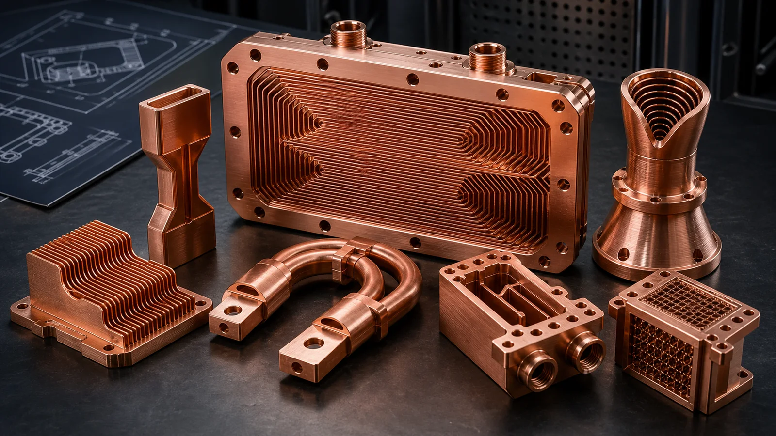
Electrical Conductivity in 3D Printed Copper Parts
A practical engineering guide to electrical conductivity in 3D printed copper parts, covering material choice, current paths, contact resistance, surface finish, heat treatment, inspection, and RFQ inputs.
Working on a copper part? Start a project review — share a brief; CAD can follow.
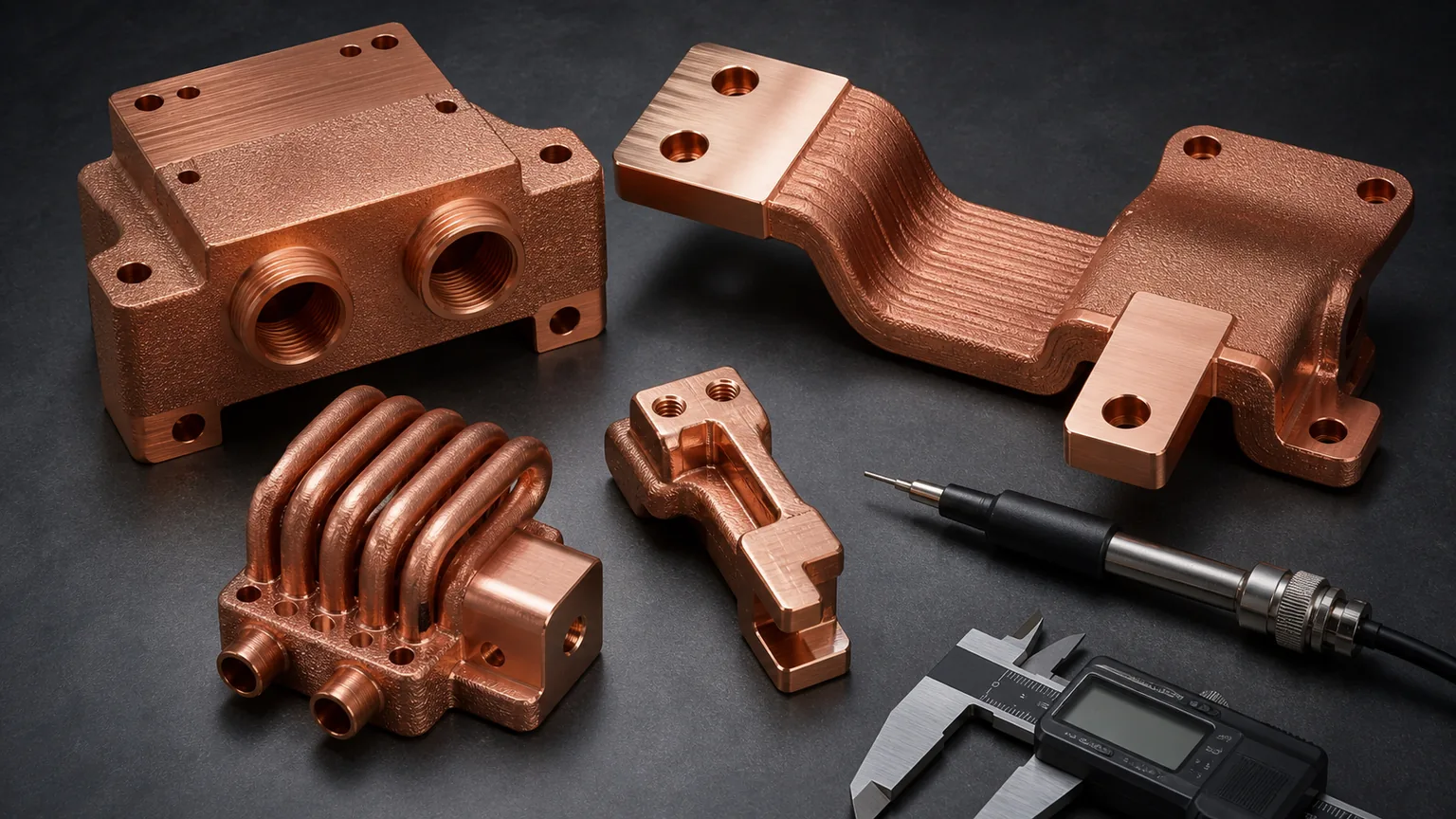
Electrical conductivity in a 3D printed copper part is not only a material property. The finished current path depends on alloy choice, density, heat treatment, surface finish, contact geometry, machining allowance, plating, cleaning, and how the part will be tested after post-processing.
Copper additive manufacturing is often requested for one simple reason: copper conducts electricity well. That is true, but it is not enough to make a good RFQ or a reliable finished component.
A printed copper busbar can have a high-conductivity alloy and still run hot because the contact pads are rough, the current path is too narrow at a bend, or the clamping face was not machined flat. A printed induction coil can use copper for its electrical path and still fail because internal cooling channels trap powder or the coil turns are too close to clean and inspect. A semiconductor or RF part can meet geometric intent and still need polishing, plating, vacuum cleaning, or documented conductivity checks before it is useful.
For that reason, conductivity should be treated as a finished-part requirement, not a powder specification alone.
Why Conductivity Questions Are Increasing
Electrical and thermal hardware are becoming more compact. AI servers, power electronics, semiconductor tools, RF systems, battery hardware, and industrial power modules are all pushing copper parts toward higher current density, tighter packaging, and more integrated cooling.
The useful engineering question is what “conductive enough” means for the delivered part. Define the permitted temperature rise and losses, the current and duty cycle, the contact interfaces and the final material state. A change in any of these can alter the decision even when the alloy name stays the same.
Public copper AM material pages point in the same direction. EOS positions copper additive manufacturing around thermal and electrical conductivity, electronics, heat exchangers, power electronics heat sinks, rocket propulsion, and copper coils. Eplus3D lists copper and CuCrZr for applications including heat exchangers, induction coils, high-frequency electronics, tooling, and electronics. 3D Systems positions CuCr1Zr(A) as a copper alloy route for heat management and conductive components where strength also matters.
The common pattern is clear: copper AM is valuable when conductivity and geometry need to work together. It is weaker when the request is only “make this in copper” with no current, contact, heat, or inspection definition.
Bulk Conductivity Is Only The First Gate
Engineers often ask for a conductivity percentage such as “%IACS.” That number matters, but it is only one layer of the finished-part problem.
For copper AM, bulk conductivity is affected by:
| Factor | Why it changes conductivity or resistance | RFQ implication |
|---|---|---|
| Material route | Pure copper, CuCrZr, and CuCr1Zr do not trade conductivity and strength the same way | Name acceptable materials and the property that matters most |
| Density and porosity | Lack of fusion, pores, and oxide films can raise resistance and reduce repeatability | Ask for density evidence or supplier route evidence when critical |
| Heat treatment | CuCrZr and CuCr1Zr properties depend on the processed state | Define whether conductivity, hardness, or strength is the priority |
| Build orientation | Layer direction can affect surface quality, supports, machining stock, and local resistance | Tie orientation to contact pads and machining strategy |
| Surface finish | Rough contact pads increase contact resistance even if the bulk material is conductive | Specify machined, polished, or plated contact surfaces |
| Geometry | Narrow necks, sharp bends, thin walls, and small radii concentrate current and heat | Review current density through the real cross-section, not nominal area |
| Temperature | Copper resistance rises with operating temperature | Provide steady-state and transient current/thermal data |
If the part is a simple flat conductor, CNC machining from copper bar may be the lower-risk route. Copper AM becomes more interesting when geometry creates value: integrated cooling, compact routing, part consolidation, complex busbar paths, conformal coils, internal channels, or combined thermal and electrical functions. For the broader route decision, see When Copper 3D Printing Is Better Than CNC Machining.
Choose Material By Failure Mode
The material decision should start with the most expensive failure mode.
Pure Copper
Pure copper is usually considered when maximum conductivity is the leading requirement. It is attractive for high-current conductors, RF or microwave surfaces, induction components, heat spreaders, and thermal hardware where mechanical loads are controlled.
The trade-off is manufacturability and finished-part robustness. Pure copper is difficult to process by standard infrared laser routes because high reflectivity and high thermal conductivity reduce process-window margin. It may also need careful handling around thin walls, threads, and clamped interfaces. If the part has critical threaded ports, repeated bolt loading, or pressure features, the highest nominal conductivity may not produce the most reliable finished part.
Use pure copper when:
- Conductivity dominates the design.
- Mechanical stress is modest or handled by thicker sections.
- Contact pads and datums can be machined after printing.
- The supplier has a validated pure copper route and inspection evidence.
When the RFQ is specifically about pure copper rather than the broader conductivity problem, use Pure Copper 3D Printing: Applications, Benefits, and Manufacturing Challenges to review applications, LPBF process limits, validation evidence, and when CuCrZr or CuCr1Zr may reduce finished-part risk. If the request has already narrowed to connector bodies, contact blocks, busbar transitions, electrodes, or machined contact pads, use Pure Copper Additive Manufacturing for Conductive Components to define the component-level current path and acceptance scope.
CuCrZr
CuCrZr is often selected when the part needs a balance of conductivity, strength, thermal stability, and machinability. It can be useful for cooled busbars, threaded conductors, mold inserts, high-heat-flux hardware, and parts that need stronger ports or clamped faces.
The important point is that CuCrZr is a processed material state, not just a label. Heat treatment, aging route, final machining sequence, and witness coupons can all matter. For this decision, use Heat Treatment for CuCrZr 3D Printed Components and Pure Copper vs CuCrZr for 3D Printed Heat Transfer Parts as companion pages.
Use CuCrZr when:
- Threads, ports, clamp loads, or thin pressure features need reserve.
- Final conductivity is important but not the only property.
- The part will be aged or heat treated under a controlled supplier route.
- You need a more robust finished component instead of the highest possible conductivity number.
CuCr1Zr
CuCr1Zr and adjacent copper-chromium-zirconium routes are common in industrial discussions because they target conductive parts with improved mechanical performance. Treat them as supplier-specific routes unless the drawing, standard, and qualification plan name the exact material. Do not assume that CuCrZr, CuCr1Zr, and pure copper are interchangeable.
For a full material comparison, start with Copper Alloy Selection for Metal 3D Printing: Pure Cu vs CuCrZr vs CuCr1Zr.
Contact Resistance Can Dominate The Result
In high-current copper parts, the failure is often not in the printed bulk. It is at the contact interface.
Contact resistance depends on real contact area, surface roughness, flatness, oxide condition, plating, clamping pressure, joint stack-up, and temperature. A printed copper conductor with a rough as-built pad can lose the advantage of copper if the joint only touches on a few peaks. A polished or machined pad can perform very differently from an as-built pad, even when the material is identical.
For busbars, connectors, and power distribution blocks, define:
- Contact pad size and current direction.
- Contact surface flatness and roughness target.
- Machined stock allowance on pads.
- Plating or anti-oxidation finish, if required.
- Bolt pattern, clamp load, and washer stack.
- Allowed temperature rise at the rated current.
- Whether conductivity is tested on a coupon, the part, or both.
This is why finishing is not cosmetic. For conductive hardware, finishing is part of the electrical design. Use Copper 3D Printing Surface Finish: As-Built, Machined, and Polished Options and Plating and Finishing Copper AM Parts before specifying contact faces or RF surfaces.
Geometry Controls Current Density
Additive manufacturing can create conductor geometry that is difficult to machine: compact bends, integrated mounts, internal cooling, complex coil paths, manifolds, and combined thermal-electrical structures. That freedom is useful only when the current path remains continuous and inspectable.
Watch for these common geometry risks:
| Geometry feature | Conductivity risk | Better RFQ instruction |
|---|---|---|
| Sharp inside bend | Current crowding and local heating | Use larger radii and verify current density |
| Thin neck near a mounting hole | Local resistance and mechanical weakness | Define minimum conductive cross-section |
| As-built contact pad | High contact resistance | Add machining stock and surface finish target |
| Internal cooling channel under conductor | Powder removal and leak risk | Define channel access, cleaning, CT, and leak test |
| Dense induction coil turns | Cleaning, insulation, and spacing problems | Define turn spacing, insulation strategy, and cooling |
| Threaded electrical terminal | Soft or rough threads after AM | Define post-machining and material state |
If the part contains internal cooling, connect the electrical RFQ to the fluid RFQ. A cooled busbar, induction coil, or conductor block should include coolant, pressure, pressure drop, leak test, and cleaning requirements. For channel-heavy parts, use Powder Removal Challenges in Copper 3D Printed Internal Channels and Tolerances and Dimensional Accuracy in Copper Metal 3D Printing.
Application-Specific Conductivity Questions
Busbars And Power Distribution Blocks
For busbars, the quotation needs more than nominal current. Provide continuous current, peak current, duty cycle, allowable temperature rise, contact requirements, insulation clearances, coolant if any, and mounting constraints.
3D printing is most useful when the busbar also needs integrated cooling, complex routing, compact packaging, or part consolidation. If it is a flat conductor with drilled holes, conventional copper machining or stamping may be better. For adjacent RFQ details, see Copper Busbars and Induction Coils RFQ Guide and Data Center Copper Busbars and Cooling Manifolds.
Induction Coils
Induction coils depend on conductivity, cooling, geometry, spacing, and surface quality. Copper AM can help when the coil needs nonstandard routing, integrated cooling, or compact turns that cannot be fabricated cleanly from tube or machined assemblies.
The RFQ should include frequency range, current, duty cycle, cooling media, pressure, insulation plan, turn spacing, and acceptance tests. If channels are integrated, powder removal and leak testing become part of the electrical design.
Electrodes
Printed copper electrodes are attractive when complex internal flushing, custom geometry, or low-volume iteration matters. However, electrodes are sensitive to surface condition, wear, dimensional repeatability, and edge definition.
For high-voltage electrodes, field concentration and surface finish can matter as much as conductivity. For EDM electrodes, wear and accuracy can dominate. Use 3D Printed Copper High-Voltage Electrodes and 3D Printed Copper EDM Electrode Failures before choosing AM only because the part is copper.
RF, Microwave, And Semiconductor Parts
RF and semiconductor equipment parts often need conductivity, thermal control, cleanliness, vacuum compatibility, machined sealing lands, and surface finish at the same time. A printed RF cavity or waveguide may need polishing or plating. A semiconductor conductor may need clean interfaces, leak testing, and dimensional stability.
Relevant companion pages include 3D Printed Copper RF Waveguide and Vacuum Parts, Copper AM Parts for Semiconductor Equipment, and the Copper AM Vacuum Manifold Design Review.
How To Specify Conductivity Testing
The test method should match the risk.
For early feasibility, a coupon tested with the same material route may be enough. For qualification-sensitive hardware, the coupon should match build orientation, heat treatment, and post-processing. For contact-critical parts, coupon conductivity does not prove joint performance. You may need contact resistance checks, temperature-rise testing, or a functional current test.
When conductivity is a supplier-approval gate rather than only a design input, use the copper LPBF supplier qualification guide for conductivity-critical parts to connect the exact process route, measurement method, coupon pedigree, finished interfaces, and repeat-build controls.
For a build-specific witness strategy, the copper AM qualification coupon guide separates specimen placement, orientation, heat-treatment state, conductivity method, traceability, and the part-level evidence that a passing coupon cannot replace.
Useful test inputs:
- Required conductivity target and test method.
- Material state at testing: as-built, stress-relieved, aged, machined, plated, or assembled.
- Whether the result is from a witness coupon, a cut-up coupon, or a finished feature.
- Number of samples and lot traceability.
- Acceptance rule for contact resistance or temperature rise, if relevant.
- Surface condition during test: bare copper, plated, polished, oxidized, cleaned, or assembled.
If the part is CuCrZr, do not test a coupon before heat treatment and assume the finished part has the same property. If contact resistance matters, do not test only bulk conductivity and ignore the interface. For broader acceptance planning, use Post-Processing Methods for 3D Printed Copper Parts and Engineering Checklist for Copper 3D Printed Part Quotation.
RFQ Checklist For Conductive Copper AM Parts
Include these items before asking for a quote:
- CAD model and 2D drawing with contact surfaces marked.
- Target material set: pure copper, CuCrZr, CuCr1Zr, or supplier recommendation allowed.
- Continuous current, peak current, duty cycle, and operating temperature.
- Maximum allowed temperature rise or resistance target.
- Contact pad flatness, roughness, plating, and clamping requirements.
- Minimum conductive cross-section or current density limit in critical regions.
- Internal cooling requirements, if any: coolant, flow, pressure, pressure drop, leak test.
- Insulation, creepage, clearance, or dielectric requirements, if relevant.
- Heat treatment and material-state evidence required.
- Conductivity, contact resistance, dimensional, and surface inspection requirements.
- Quantity, revision status, and lead time.
If these inputs are not available, the first quote will include more uncertainty. That uncertainty usually appears as broader assumptions, extra clarification cycles, or conservative pricing for machining, polishing, plating, testing, and rework.
When Copper AM Is A Good Fit
Copper AM is a strong candidate when the part needs at least one of these:
- Electrical conduction plus integrated cooling.
- Complex current routing in a compact envelope.
- Consolidation of conductor, manifold, mounting, and thermal features.
- Low-volume or prototype conductive hardware with high geometry value.
- RF, vacuum, or semiconductor copper hardware where internal geometry matters.
- Induction or electrode geometry that is difficult to fabricate conventionally.
It is usually a weak fit when the part is a flat, simple copper plate; when contact pads can be made faster by machining; when conductivity is the only requirement; or when the design has no inspection plan for current path, surface finish, and material state.
Practical Verdict
For conductive copper parts, do not ask only “What conductivity can you print?”
Ask:
- What finished material state will the part be delivered in?
- Which surfaces carry current, and how will they be machined or finished?
- Where is the highest current density?
- Does the part need cooling, cleaning, leak testing, or plating?
- How will conductivity or contact resistance be verified?
That is the difference between a copper AM marketing request and a quotable engineering package.
If you are preparing a conductive copper AM RFQ, send the CAD model, drawing, quantity, current profile, material preference, contact requirements, surface finish targets, cooling data if any, and inspection requirements to info@szcomo.com. The fastest review path is a drawing package that separates bulk conductivity, contact surfaces, thermal limits, and final acceptance evidence.
Copper AM quotation
Need to choose a copper material for a part?
Describe the part, operating environment, and properties that matter. State the material preference only if decided; material state and acceptance can be reviewed together.
NDA available on request. We reply within 2 business days.
Before you submit: Copper materials and delivered condition.